

Today we’re starting a series of articles that will explain the principles of SSD performance testing and how to interpret the results of such tests.
Information gathered in those articles is also meant to give a better understanding of SSD performance test results to end users that need to assess the capabilities of SSDs. Measuring and assessing performance of SSD devices is not an easy task and it requires a lot of time and effort to produce accurate results. This is important because only accurate results allow users to compare the performance of various products available on the market. This article might be of some help in projecting the whole data storage environments, especially with all-flash storage where the server uses only SSD disks. Read the first part of the SSD series.
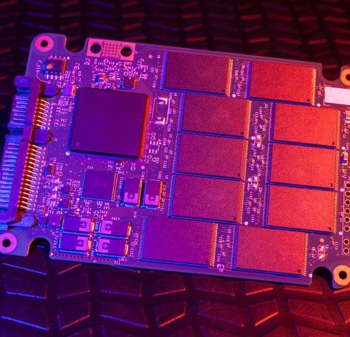
How does flash memory work? Recap on SSD
SSD devices tend to change performance levels in response to the previously written data, which means that SSD drive may show different performance in same test because it was exposed to different workload before performing particular test. This is mostly related to the fact that SSDs slow down after writing some amount of data on them – usually it requires to write whole or most of disk capacity. However, it doesn’t actually require to fill SSD, it rather requires to perform as many writes to a disk as it is needed to fill its capacity. SSD in all cases will deliver lower performance after some time in comparison to its state fresh out of the box
Before I will dive into basics of SSDs performance testing I would like to explain the basic principles on how actually flash memory operates. This knowledge is important in order to understand why the performance of SSD drives decrease after issuing writes to them.
Basic part used in flash memory is the data cell which is a transistor. Flash memory uses similar principle of operation to DRAM but it is of course non volatile. This goal is achieved thanks the to so called floating gate transistor. This kind of transistor doesn’t have to get its source from capacitor (as DRAM does), it is capable of storing some charge trapped in the gate (transistor input). It operates in such way that applying some low voltage (read voltage) to the gate causes the current one to flow only if the gate doesn’t store a charge. When the charge is stored in the gate, low voltage is not enough to cause the current flow. This shows that a cell represents binary 1 when it is not charged, and binary 0 if it is charged. Moreover, those floating gate transistors have also ability to conduct (turn on) when voltage over some threshold is applied to them. This voltage is higher than the one used to read data from those cells.
Flash memory is basically made out of those floating gate transistors – cells that store data. Those cells are organized into pages that usually are 2K, 4K, 8K or 16K in size. Pages are organized into blocks that usually contain 128 or 256 pages. Block is a grid with pages arranged as a rows on that grid. Most commonly used NAND flash memory wires up each page in a block in series. Output (drain of transistor) of one page is plugged into source of transistor in following page. In this arrangement of pages data is read or written (but not overwritten – will be explained later) only from one page at a time. In order to perform read, lower voltage is applied to the gates of page that is being read and higher voltage is applied to cells in other pages. Because this higher voltage turns on cells, data that is read from given page (using read voltage) simply travels down through the grid and is accessed. Writing data to the page is made by applying high voltage to the cells gates in particular page while grounding output of those cells for whole grid (block). Only columns with cells that have to be charged are grounded. During this process the charge is trapped in the floating gate of a cell and it stores binary 0.
Page is the smallest piece of flash memory that can be read or written. However, it isn’t possible to overwrite single page, it is only possible to overwrite the whole block. The process of clearing cells requires high voltage, its level is so high that trying to clear single page might affect pages that are nearby. Simply speaking, trying to clear a single page (row in a grid) requires to apply voltage this high that it may change the charge of the cells on other pages of a given block. This obviously will lead to data corruption that is not acceptable. This is the reason why it is possible to read and write data from single page but process of overwriting (or clearing) data is possible only on block level.
To sum up, flash memory is organized into pages that forms blocks. It is possible to read and write data from a single page but it is not possible to overwrite data in a single page, it is required to clear whole block and write data back to that block.
Stay tuned – to be continued!


Leave a Comment